Can Printed Circuit Board Assembly Withstand Harsh Environments?
Printed Circuit Board Assembly Withstand Harsh Environments
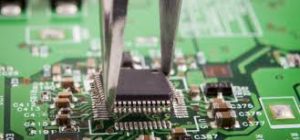
A printed circuit board is a key part of any electronic product. Its purpose is to connect all the components and power them so they can perform their intended tasks. However, PCBs can be subjected to a wide range of harsh environments that can hinder their performance and lead to malfunctioning or even catastrophic failure. These environments include a buildup of moisture and dust, corrosive elements like sulfur and salt spray, electromagnetic interference (EMI), intense mechanical vibrations and more.
A typical printed circuit board assembly is made of water-resistant FR-4 fiberglass with copper layers and components soldered onto them. These materials are capable of handling high temperatures, but there are limits beyond which the PCB can be damaged or degraded. One important consideration is the melting point of the solder used to attach components. This must not be exceeded or the connections can break. The other is the glass transition temperature (Tg), which is the maximum temperature at which the copper material begins to degrade and lose its conductivity. This limit is also known as the “decomposition temperature.”
Extremes of temperature are another common challenge for a PCB. They must be able to operate in temperatures from freezing to very hot and even high altitudes where the air is thin and has a low humidity. The PCB can be designed with thermal management circuitry and/or heat sinks to ensure it stays operational in the appropriate temperature range.
Can Printed Circuit Board Assembly Withstand Harsh Environments?
The harshest of environmental conditions are those involving moisture, corrosion and contaminating elements. Creep corrosion is caused by excess sulfur in the work environment and can quickly damage a PCB’s internal components, making them unusable. A simple solution is to remove the sulfur source from the work area whenever possible. In addition, a special specialized test that has been developed in recent years is now available to assess a PCB’s susceptibility to creep corrosion.
Other contaminants are a concern as well. Salt spray and fungus can be harmful to the internal components on a PCB, as can a buildup of moisture that can cause signal attenuation or short circuits leading to a fire risk in extreme cases. Electrostatic discharge (ESD) from lightning or other electrical sources can also destroy the electronic parts on a circuit board. In addition to proper design, a PCB that must endure harsh environments should be encased or covered in conformal coating to keep moisture and contaminants away from the internal components.
In some cases, a PCB may be subjected to the additional demands of military-grade requirements. This requires stricter standards for a PCB’s layout, manufacturing processes and materials. For instance, there are standards like MIL-PRF-31032 that dictate how a PCB can withstand the effects of gamma radiation.
Regardless of the environment a PCB must be able to withstand, Altest provides a wide variety of value-added services that can help ensure it is ready for the task at hand. This includes a DFM check that validates the PCB’s design for manufacturing, reviews component spacing, pin indications, footprint corroboration and more. This helps reduce the likelihood of errors during the assembly process that could result in costly delays and RMAs.