The Role of Microvias in HDI PCBs
Microvias in HDI PCBs
Whether used in smartphones, medical devices or aerospace applications, microvias play an important role in the success of electronic innovations. Understanding the different types of these vias and their responsibilities in PCB design is crucial for designers to ensure proper use and high reliability.
Microvias are small holes in the circuit board that connect layers to improve routing capabilities and increase circuit density. They are often filled with copper and provide a reliable connection for signal paths. These features also reduce the amount of space required for components and lower overall fabrication costs. Microvias are most commonly drilled by laser and can be categorized into two types: blind and buried. They can be fabricated with different substrate materials, plating methods and surface finishes.
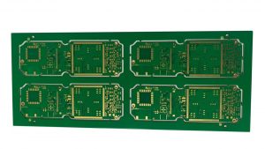
Blind and buried vias are most common in hdi pcb. These are drilled using laser technology and have a diameter of around 50 microns or less. The smaller diameters and precise hole locations offered by this technology allow for more interlayer connections with fewer layers in a design. They are typically filled with copper and can be plated with different metals such as immersion tin, gold or ENEPIG.
The Role of Microvias in HDI PCBs
When compared to traditional through-hole vias, the smaller size of microvias enables more routing channels on each layer, which significantly increases the circuitry and components that can be packed into a single PCB. This allows for higher performance in end products, such as faster speeds and improved noise reduction. The tighter trace spacing and thinner dielectric materials associated with microvias also enhance signal speed and minimize interference or crosstalk, resulting in superior signal integrity.
One of the most critical steps in designing a microvia-based PCB is to determine the layer count and the dielectric thicknesses needed for the project. This will help the designer to properly design vias that meet the minimum aspect ratio limits, as well as maintain a reasonable routing density between layer pairs.
Another key step is to select the best design for the signal traces that will be routed through the microvias. This process requires careful consideration of the signal speed and impedance requirements of each component. Proper design of the signal traces will ensure efficient communication between layers and will limit current flow, which can cause failures.
One of the key features of HDI PCBs is the utilization of microvias, which are tiny holes drilled into the PCB substrate to create electrical connections between different layers of the board. Unlike through-hole vias or conventional vias, which have larger diameters and require more space, microvias have diameters as small as 0.1mm or less, allowing for densely packed interconnections and intricate routing paths. By incorporating microvias, HDI PCBs enable designers to achieve higher routing densities, shorter signal paths, and improved signal integrity, ultimately leading to enhanced performance and reliability in electronic devices.
As the manufacturing industry continues to develop new technologies, the demand for higher performance and smaller boards will grow. HDI provides a great solution to these demands, offering a wide range of benefits that can significantly enhance a product’s functionality and reduce the time it takes to bring it to market. By utilizing microvias, manufacturers can offer their customers high-density circuit boards with the same level of performance and reliability that they are accustomed to.